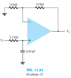
Question: Calculate the cutoff frequency of a first-
Calculate the cutoff frequency of a first-order low-pass filter in the circuit of Fig. 11.57.
> What frequency range results in the circuit of Fig. 13.23 for
> Calculate the center frequency of a VCO using a 566 IC as in Fig. 13.22 for
> Sketch the input and output waveforms for a one-shot using a 555 timer triggered by a 10-kHz clock for
> Draw the circuit of a one-shot using a 555 timer to provide one time period of 20ms. If What value of C is needed?
> Sketch the circuit of a 555 timer connected as an astable multivibrator for operation at 350 kHz. Determine the value of capacitor C needed using
> What is the maximum count interval using a 12-stage counter operated at a clock rate of 20 MHz?
> How many count steps occur using a 12-stage digital counter at the output of an ADC?
> For a dual-slope converter, describe what occurs during the fixed time interval and the count interval.
> What voltage resolution is possible using a 12-stage ladder network with a 10-V reference voltage?
> For the voltage feedback network of Fig. 4.130, determine: a. IC. b. VC. c. VE. d. VCE.
> Draw the diagram of a 741 op-amp operated from {15-V supplies with Vi (-) = V and Vi (+) = + 5 V. Include terminal pin connections.
> Calculate the efficiency of the circuit of Problem 8 if the bias current is ICQ = 150 mA.
> A transformer-coupled class A amplifier drives a 16-Ω speaker through a 3.87:1 transformer. Using a power supply of VCC = 36 V, the circuit delivers 2 W to the load. Calculate: a. P(ac) across transformer primary. b. VL (ac). c. V(ac) at transformer prim
> Calculate the transformer turns ratio required to connect four parallel 16-Ω speakers so that they appear as an 8-kΩ effective load.
> What turns ratio transformer is needed to couple to an 8-Ω load so that it appears as an 8-kΩ effective load?
> A class A transformer-coupled amplifier uses a 25:1 transformer to drive a 4-Ω load. Calculate the effective ac load (seen by the transistor connected to the larger turns side of the trans- former).
> If the circuit of Fig. 12.35 is biased at its center voltage and center collector operating point, what is the input power for a maximum output power of 1.5 W?
> What maximum output power can be delivered by the circuit of Fig. 12.35 if RB is changed to 1.5 kΩ?
> What maximum power can a silicon transistor (TJmax = 200°C) dissipate into free air at an ambient temperature of 80°C?
> A 160-W silicon power transistor operated with a heat sink (uSA = 1.5°C>W) has uJC = 0.5°C>W and a mounting insulation of uCS = 0.8°C>W. What maximum power can be handled by the transistor at an ambient temperature of 80°C? (The junction temperature shou
> For the network of problem 27 a. Determine ICQ using the equation ICQ b. Compare with the results of problem 27 for ICQ. c. Compare R’ to RF/. d. Is the statement valid that the larger R’ is compa
> Determine the maximum dissipation allowed for a 100-W silicon transistor (rated at 25°C) for a derating factor of 0.6 W>°C at a case temperature of 150°C.
> For distortion readings of D2 = 0.15, D3 = 0.01, and D4 = 0.05, with I1 = 3.3 A and RC = 4 Ω, calculate the total harmonic distortion fundamental power component and total power.
> Calculate the second harmonic distortion for an output waveform having measured values of VCEmin = 2.4 V, VCEQ = 10 V, and VCEmax = 20 V.
> Calculate the total harmonic distortion for the amplitude components of Problem 19.
> Calculate the input power dissipated by the circuit of Fig. 12.35 if RB is changed to 1.5 kΩ.
> Calculate the harmonic distortion components for an output signal having fundamental amplitude of 2.1 V, second harmonic amplitude of 0.3 V, third harmonic component of 0.1 V, and fourth harmonic component of 0.05 V.
> For the power amplifier of Fig. 12.37, calculate: a. Po(ac). b. Pi(dc). c. %h. d. Power dissipated by both output transistors.
> If the input voltage to the power amplifier of Fig. 12.36 is 8-V rms, calculate: a. Pi(dc). b. Po(ac). c. %h. d. Power dissipated by both power output transistors.
> For the class B power amplifier of Fig. 12.36, calculate: a. Maximum Po(ac). b. Maximum Pi(dc). c. Maximum %h. d. Maximum power dissipated by both transistors.
> Sketch the circuit diagram of a quasi-complementary amplifier, showing voltage waveforms in the circuit.
> For the collector-feedback configuration of Fig. 4.129, determine: a. IB. b. IC. c. VC.
> Calculate the efficiency of a class B amplifier for a supply voltage of VCC = 22 V driving a 4-Ω load with peak output voltages of: a. VL(p) = 20 V. b. VL(p) = 4 V.
> For a class B amplifier with VCC = 25 V driving an 8-Ω load, determine: a. Maximum input power. b. Maximum output power. c. Maximum circuit efficiency.
> For a class B amplifier providing a 22-V peak signal to an 8-Ω load and a power supply of VCC = 25 V, determine: a. Input power. b. Output power. c. Circuit efficiency.
> Draw the circuit diagram of a class B npn push–pull power amplifier using transformer- coupled input.
> Draw the circuit diagram of a class A transformer-coupled amplifier using an npn transistor.
> Calculate the input and output power for the circuit of Fig. 12.35. The input signal results in a base current of 5 mA rms.
> Show the connection (including pin information) of an LM124 IC stage connected as a unity- gain amplifier.
> Determine the output voltage for the circuit of Fig. 11.52.
> Determine the output voltage for the circuit of Fig. 11.51.
> Calculate the output voltage for the circuit of Fig. 11.50 with inputs of V1 = 40 mV rms and V2 = 20 mV rms.
> a. Repeat parts (a) through (e) of Problem 25 for the network of Fig. 4.128. Change to 180 in part (b). b. What general conclusions can be made about networks in which the condition RE > 10R2 is satisfied and the quantities IC and VCE are to be determ
> Show the connection of two op-amp stages using an LM358 IC to provide outputs that are 15 and —30 times larger than the input. Use a feedback resistor, RF = 150 kΩ, in all stages.
> Show the connection of an LM124 quad op-amp as a three-stage amplifier with gains of +15, —22, and —30. Use a 420-kΩ feedback resistor for all stages. What output voltage results for an input of V1 = 80 mV?
> Calculate the output voltage in the circuit of Fig. 11.49.
> Calculate the output voltage of the circuit of Fig. 11.48 for an input of 150 mV rms.
> Calculate the lower and upper cutoff frequencies of the bandpass filter circuit in Fig. 11.59.
> Calculate the cutoff frequency of the high-pass filter circuit in Fig. 11.58.
> Calculate Vo in the circuit of Fig. 11.56.
> Calculate the output current Io in the circuit of Fig. 11.55.
> Calculate Vo for the circuit of Fig. 11.54.
> a. Determine IC and VCE for the network of Fig. 4.125. b. Change  to 120 (50% increase), and determine the new values of IC and VCE for the net- work of Fig. 4.125. c. Determine the magnitude of the percentage change in IC and VCE using
> For the circuit of Fig. 11.53, calculate IL.
> Show the connection (including pin information) of two LM358 stages connected as unity-gain amplifiers to provide the same output.
> Calculate the output voltage for the circuit of Fig. 11.47 for an input of Vi = 3.5 mV rms.
> Calculate the output voltage of the circuit in Fig. 10.68 for Rf = 68 kΩ.
> Calculate the output voltage developed by the circuit of Fig. 10.68 for Rf = 330 kΩ.
> What range of output voltage is developed in the circuit of Fig. 10.67?
> What input must be applied to the input of Fig. 10.66 to result in an output of 2.4 V?
> What output voltage results in the circuit of Fig. 10.66 for an input of V1 = —0.3 V?
> What is the range of the output voltage in the circuit of Fig. 10.65 if the input can vary from 0.1 to 0.5 V?
> What input voltage results in an output of 2 V in the circuit of Fig. 10.64?
> a. Using the characteristics of Fig. 4.121, determine RC and RE for a voltage-divider network having a Q-point of ICQ = 5 mA and VCEQ = 8 V. Use VCC = 24 V and RC = 3RE. b. Find VE. c. Determine VB. d. Find R2 if R1 = 24 kΩ assuming that RE 10R2. e. C
> Determine the output voltage of an op-amp for input voltages of Vi1 = 200 mV and Vi2 = 140 mV. The amplifier has a differential gain of Ad = 6000 and the value of CMRR is: a. 200. b. 105.
> Calculate the CMRR (in dB) for the circuit measurements of VD = 1 mV, VO = 120 mV, VC = 1 mV, and VO = 20 mV.
> For the typical characteristics of the 741 op-amp, calculate the following values for the circuit of Fig. 10.75: a. ACL. b. Zi. c. Zo.
> Using the specifications listed in Table 10.3; calculate the typical offset voltage for the circuit connection of Fig. 10.75.
> For an input of V1 = 50 mV in the circuit of Fig. 10.75, determine the maximum frequency that may be used. The op-amp slew rate SR = 0.4 V>ms.
> What is the range of the voltage-gain adjustment in the circuit of Fig. 10.63?
> For an op-amp having a slew rate of SR = 2.4 V>ms, what is the maximum closed-loop volt- age gain that can be used when the input signal varies by 0.3 V in 10 ms?
> Determine the cutoff frequency of an op-amp having specified values B1 = 800 kHz and AVD = 150 V>mV.
> Calculate the input bias current at each input of an op-amp having specified values of IIO = 4 nA and IIB = 20 nA.
> Calculate the total offset voltage for the circuit of Fig. 10.75 for an op-amp with specified values of input offset voltage VIO = 6 mV and input offset current IIO = 120 nA.
> a. Determine ICQ, VCEQ, and IBQ for the network of Problem 15 (Fig. 4.125) using the approxi- mate approach even though the condition established by Eq. (4.33) is not satisfied. b. Determine ICQ, VCEQ, and IBQ using the exact approach. c. Compare solutio
> Calculate VO in the circuit of Fig. 10.74.
> Calculate the output voltage, VO, in the circuit of Fig. 10.73.
> Calculate the output voltages V2 and V3 in the circuit of Fig. 10.72.
> Calculate the output voltage for the circuit of Fig. 10.71.
> What output voltage results in the circuit of Fig. 10.70 for V1 = +0.5 V?
> Sketch the output waveform resulting in Fig. 10.69.
> What is the output voltage in the circuit of Fig. 10.62?
> If the applied ac power to a system is 5 mW at 100 mV and the output power is 48 W, determine: a. The power gain in decibels. b. The voltage gain in decibels if the output impedance is 40 kΩ. c. The input impedance. d. The output voltage.
> a. The total decibel gain of a three-stage system is 120 dB. Determine the decibel gain of each stage if the second stage has twice the decibel gain of the first and the third has 2.7 times the decibel gain of the first. b. Determine the voltage gain of
> Input and output voltage measurements of VI = 10 mV and VO = 25 V are made. What is the voltage gain in decibels?
> Repeat Problem 21 using the exact (Thévenin) approach and compare solutions. Based on the results, is the approximate approach a valid analysis technique if Eq. (4.33) is satisfied?
> Two voltage measurements made across the same resistance are V1 = 110 V and V2 = 220 V. Calculate the power gain in decibels of the second reading over the first reading.
> Determine GdBm for an output power level of 25 W.
> Calculate the power gain in decibels for each of the following cases. a. Po = 100 W, Pi = 5 W. b. Po = 100 mW, Pi = 5 mW. c. Po = 100 mW, Pi = 20 mW.
> The application of a 10-mV, 100-kHz square wave to an amplifier resulted in the output wave- form of Fig. 9.90. a. Write the Fourier series expansion for the square wave through the ninth harmonic. b. Determine the bandwidth of the amplifier to the accur
> A four-stage amplifier has a lower 3-dB frequency for an individual stage of f1 = 40 Hz. What is the value of f1 for this full amplifier?
> Calculate the overall upper 3-dB frequency for a four-stage amplifier having an individual stage value of f2 = 2.5 MHz.
> Calculate the overall voltage gain of four identical stages of an amplifier, each having a gain of 20.
> Repeat the analysis of Problem 31 for the network of Fig. 9.89.
> For the network of Fig. 9.88: a. Determine gm0 and gm. b. Find Av and Avs in the mid-frequency range. c. Determine fHi and fHo. d. Sketch the frequency response for the high-frequency region using a Bode plot and determine the cutoff frequency. e. What i
> Repeat the analysis of Problem 27 for the network of Fig. 9.83 with Rs and Vs of Fig. 9.87.
> Determine the following for the voltage-divider configuration of Fig. 4.128 using the approxi- mate approach if the condition established by Eq. (4.33) is satisfied. a. IC. b. VCE. c. IB. d. VE. e. VB.
> Determine: a. 20 log10 (84) using Eq. (9.6) and compare with 20 log10 14. b. 10 log10 (1) using Eq. (9.7) and compare with 10 log10 4 * 10-3. c. log10 (40) (0.2) using Eq. (9.8) and compare with log10 8.
> Repeat the analysis of Problem 27 for the network of Fig. 9.82 with Rs and Vs of Fig. 9.86.
> Repeat the analysis of Problem 27 for the network of Fig. 9.81 with Rs and Vs of Fig. 9.85.