Question: Determine Vo for the network of Fig.
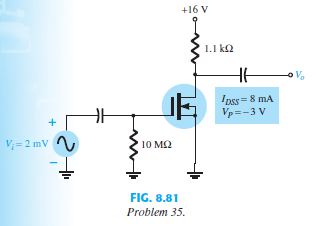
Determine Vo for the network of Fig. 8.81 if gos = 20 mS.
> Repeat the analysis of Problem 27 for the network of Fig. 9.83 with Rs and Vs of Fig. 9.87.
> Determine the following for the voltage-divider configuration of Fig. 4.128 using the approxi- mate approach if the condition established by Eq. (4.33) is satisfied. a. IC. b. VCE. c. IB. d. VE. e. VB.
> Determine: a. 20 log10 (84) using Eq. (9.6) and compare with 20 log10 14. b. 10 log10 (1) using Eq. (9.7) and compare with 10 log10 4 * 10-3. c. log10 (40) (0.2) using Eq. (9.8) and compare with log10 8.
> Repeat the analysis of Problem 27 for the network of Fig. 9.82 with Rs and Vs of Fig. 9.86.
> Repeat the analysis of Problem 27 for the network of Fig. 9.81 with Rs and Vs of Fig. 9.85.
> For the network of Fig. 9.80 with Rs and Vs of Fig. 9.84: a. Determine fHi and fHo. b. Find fb and fT. c. Sketch the frequency response for the high-frequency region using a Bode plot and deter- mine the cutoff frequency. d. What is the gain-bandwidth pr
> a. The feedback capacitance of an inverting amplifier is 10 pF. What is the Miller capacitance at the input if the gain of the amplifier is —120? b. What is the Miller capacitance at the output of the amplifier? c. Is it a good approximation to assume CM
> Repeat the analysis of Problem 23 for the network of Fig. 9.89. What effect does the voltage- divider configuration have on the input impedance and the gain Avs compared to the biasing arrangement of Fig. 9.88?
> Repeat the analysis of Problem 23 with rd = 100 kΩ. Does it have an effect of any consequence on the results? If so, which elements?
> For the network of Fig. 9.88: a. Determine VGSQ and IDQ. b. Find gm0 and gm. c. Calculate the midband gain of Av = VO>VI. d. Determine Zi. e. Calculate Avs = VO>Vs. f. Determine fLG, fLC, and fLS. g. Determine the low-cutoff frequency. h. Sketch th
> a. Determine the common logarithm of the number 0.24 × 10⁶. b. Determine the natural logarithm of the number of part (a) using Eq. (9.4). c. Determine the natural logarithm of the number of part (a) using natural logarithms and compare with the solution
> For the network of Fig. 9.80: a. Determine re. b. Find Avmid = VO>VI. c. Calculate Zi. d. Determine fLS, fLC, and fLE. e. Determine the low cutoff frequency. f. Sketch the asymptotes of the Bode plot defined by the cutoff frequencies of part (d). g. S
> a. Repeat problem 16 with = 140 using the approximate approach and compare results. b. Is the approximate approach valid?
> Using the characteristics of Fig. 6.11, determine ID for the following levels of VGS (with VDS 7 VP): a. VGS = 0 V. b. VGS = —1 V. c. VGS = —1.5 V. d. VGS = —1.8 V. e. VGS = —4 V. f. VGS = —6 V.
> Repeat the analysis of Example 9.11 with ro = 40 kΩ. What is the effect on Avmid, fLS, fLC, fLE, and the resulting cutoff frequency?
> a. What frequency is one octave above 5 kHz? b. What frequency is one decade below 10 kHz? c. What frequency is two octaves below 20 kHz? d. What frequency is two decades above 1 kHz?
> For the network of Fig. 9.79: a. Determine the mathematical expression for the angle by which VO leads VI. b. Determine the phase angle at f = 100 Hz, 1 kHz, 2 kHz, 5 kHz, and 10 kHz, and plot the resulting curve for the frequency range of 100 Hz to 10 k
> For the network of Fig. 9.79: a. Determine the mathematical expression for the magnitude of the ratio VO>VI. b. Using the results of part (a), determine Vo>Vi at 100 Hz, 1 kHz, 2 kHz, 5 kHz, and 10 kHz, and plot the resulting curve for the frequenc
> Given the characteristics of Fig. 9.78, sketch: a. The normalized gain. b. The normalized dB gain (and determine the bandwidth and cutoff frequencies). /
> a. Determine the common logarithm of the following numbers: 103, 50, and 0.707. b. Determine the natural logarithm of the numbers appearing in part (a). c. Compare the solutions of parts (a) and (b).
> For a JFET having specified values of gfs = 4.5 mS and gos = 25 mS, determine the device output impedance Zo (FET) and device ideal voltage gain Av(FET).
> A specification sheet provides the following data (at a listed drain-source current): / At the listed drain–source current, determine: a. gm. b. rd.
> Determine the value of gm for a JFET (IDSS = 8 mA, VP = - 5 V) when biased at VGSQ = VP>4.
> A JFET (IDSS = 10 mA, VP = - 5 V) is biased at ID = IDSS>4. What is the value of gm at that bias point?
> Determine the saturation current (ICsat) for the network of Fig. 4.125.
> Calculate the input impedance (Zi) and output impedance (Zo) for the amplifier circuit of Fig. 8.94.
> For the amplifier circuit of Fig. 8.94, calculate the voltage gain of each stage and the overall amplifier voltage gain.
> For the cascade amplifier of Fig. 8.94, calculate the dc bias voltages currents of each stage.
> For the cascade amplifier of Fig. 8.93, using JFETs with specifications IDSS = 12 mA, VP = - 3 V, and gos = 25 mS, calculate the circuit input impedance (Zi) and output impedance (Zo).
> If both JFETs in the cascade amplifier of Fig. 8.93 are changed to those having the specifications IDSS = 12 mA, VP = - 3 V, and gos = 25 mS, calculate the resulting voltage gain for each stage, the overall voltage gain, and the output voltage, Vo.
> If both JFETs in the cascade amplifier of Fig. 8.93 are changed to those having specifications IDSS = 12 mA and VP = - 3 V, calculate the resulting dc bias of each stage.
> For the JFET cascade amplifier of Fig. 8.93, using identical JFETs with IDSS = 8 mA and VP = - 4.5 V, calculate the voltage gain of each stage, the overall gain of the amplifier, and the output voltage Vo.
> For the JFET cascade amplifier in Fig. 8.93, calculate the dc bias conditions for the two identical stages, using JFETs with IDSS = 8 mA and VP = - 4.5 V.
> For a JFET having gm = 6 mS at VGSQ = - 1 V, what is the value of IDSS if VP = - 2.5 V?
> Design the self-bias network of Fig. 8.89 to have a gain of 10. The device should be biased at VGSQ= 1VP.
> Given the information appearing in Fig. 4.127, determine: a. IC. b. VE. c. VCC. d. VCE. e. VB. f. R1.
> Design the fixed-bias network of Fig. 8.88 to have a gain of 8.
> Determine the output voltage for the network of Fig. 8.87 if VI = 0.8 mV and rd = 40 kΩ.
> Determine Vo for the network of Fig. 8.86 if Vi = 4 mV, V GS (Th) = 4 V, and ID (on) = 4 mA, with VGS (on) = 7 V and gos = 20 mS.
> Determine VO for the network of Fig. 8.86 if VI = 20 mV.
> Repeat Problem 41 if k drops to 0.2 * 10-3. Compare results.
> Determine Zi, Zo, and Av for the amplifier of Fig. 8.85 if k = 0.3 * 10-3.
> Determine gm for a MOSFET if VGS (Th) = 3 V and it is biased at VGSQ = 8 V. Assume k = 0.3 * 10-3.
> Calculate the value of gm for a JFET (IDSS = 12 mA, VP = - 3 V) at a bias point of VGS = - 0.5 V.
> Determine Zi, Zo, and Av for the network of Fig. 8.84.
> Determine Vo for the network of Fig. 8.83 if Vi = 1.8 mV.
> Given the information provided in Fig. 4.126, determine: a. IC. b. VE. c. VB. d. R1.
> Repeat Problem 36 if rd = 25 kΩ and compare results.
> Determine Zi, Zo, and Av for the network of Fig. 8.82 if rd = 60 kΩ.
> Determine Zi, Zo, and Av for the network of Fig. 8.80.
> Repeat Problem 32 if rd = 20 kΩ and compare results.
> Determine Zi, Zo, and Av for the network of Fig. 8.79.
> Determine Zi, Zo, and Av for the network of Fig. 8.78 if rd = 30 kΩ.
> Repeat Problem 29 if rd = 20 kΩ and compare results.
> For a JFET having device parameters gm0 = 5 mS and VP = - 4 V, what is the device current at VGS = 0 V?
> Determine Zi, Zo, and Vo for the network of Fig. 8.77 if Vi = 4 mV
> a. Repeat problem 15 for = 140 using the general approach (not the approximate). b. What levels are affected the most? Why?
> Repeat Problem 26 if rd = 20 kΩ and compare results.
> Repeat Problem 25 if rd = 20 kΩ and compare results.
> Repeat Problem 25 with the capacitor CS removed and compare results.
> Determine Zi, Zo, and Vo for the network of Fig. 8.76 if Vi = 20 mV.
> Determine Zi, Zo, and Av for the network of Fig. 8.75 if IDSS = 6 mA, VP = - 6 V, and gos = 40 mS.
> a. Find the value of RS to obtain a voltage gain of 2 for the network of Fig. 8.74 using rd = ∞ Ω. b. Repeat part (a) with rd = 30 kΩ. What was the impact of the change in rd on the gain and the a
> Repeat Problem 20 if gos is 10 mS. Compare the results to those of Problem 20.
> Determine Zi, Zo, and Av for the network of Fig. 8.73 if the 20@mF capacitor is removed and the parameters of the network are the same as in Problem 20. Compare results with those of Problem 20.
> Determine Zi, Zo, and Av for the network of Fig. 8.73 if gfs = 3000 mS and gos = 50 ms.
> Determine the pinch-off voltage of a JFET with gm0 = 10 mS and IDSS = 12 mA.
> For the voltage-divider bias configuration of Fig. 4.125, determine: a. IBQ. b. ICQ. c. VCEQ. d. VC. e. VE. f. VB.
> a. Determine Zi, Zo, and Av for the network of Fig. 8.72 if IDSS = 10 mA, VP = —4 V, and rd = 20 kΩ. b. Repeat part (a) with rd = 40 kΩ. What was the impact on the results?
> a. Determine Zi, Zo, and Av for the network of Fig. 8.71 if IDSS and VP are one-half the values of Problems 17. This is IDSS = 5 mA and VP = —3 V. b. Compare the solutions to that of Problem 17.
> Determine Zi, Zo, and Av for the network of Fig. 8.71 if IDSS = 10 mA, VP = - 6 V, and rd = 40 kΩ.
> Sketch the ac equivalent model for a JFET if IDSS = 10 mA, VP = - 4 V, VGSQ = - 2 V, and gos = 25 mS.
> Sketch the ac equivalent model for a JFET if gfs = 5.6 mS and gos = 15 mS.
> a. Plot gm versus VGS for an n-channel JFET with IDSS = 12 mA and VP = - 6 V. b. Plot gm versus ID for the same n-channel JFET as part (a).
> For a 2N4220 n-channel JFET [gfs (minimum) = 750 mS, gos (maximum) = 10 mS]: a. What is the value of gm? b. What is the value of rd?
> Using the drain characteristic of Fig. 8.70: a. What is the value of rd for VGS = 0 V? b. What is the value of gm0 at VDS = 10 V?
> Using the transfer characteristic of Fig. 8.69: a. What is the value of gm0? b. Determine gm at VGS = - 0.5 V graphically. c. What is the value of gm at VGSQ = - 0.5 V using Eq. (8.6)? Compare with the solution to part (b). d. Graphically determine gm at
> If a JFET having a specified value of rd = 100 kΩ has an ideal voltage gain of Av (FET) = - 200, what is the value of gm?
> For the network of Fig. 5.153, what value of RC will cut the voltage gain to half the value obtained in problem 13?
> Calculate gm0 for a JFET having device parameters IDSS = 12 mA and VP = - 4 V.
> Given the measurement VS = 1.7 V for the network of Fig. 7.82, determine: a. IDQ. b. VGSQ. c. IDSS. d. VD. e. VDS.
> For the network of Fig. 7.81, determine: a. VGSQ and IDQ. b. VDS, VD, VG, and VS.
> Determine IDQ for the network of Fig. 7.80 using a purely mathematical approach. That is, establish a quadratic equation for ID and choose the solution compatible with the network characteristics. Compare to the solution obtained in Problem 6.
> For the self-bias configuration of Fig. 7.80: a. Sketch the transfer curve for the device. b. Superimpose the network equation on the same graph. c. Determine IDQ and VGSQ. d. Calculate VDS, VD, VG, and VS.
> Determine VD and VGS for the fixed-bias configuration of Fig. 7.79.
> Determine VD and VGS for the fixed-bias configuration of Fig. 7.78.
> Repeat Problem 16 using the universal JFET bias curve.
> Repeat Problem 12 using the universal JFET bias curve.
> Repeat Problem 1 using the universal JFET bias curve.
> Using the characteristics of Fig. 4.121, determine the following for an emitter-bias configura- tion if a Q-point is defined at ICQ = 4 mA and VCEQ = 10 V. a. RC if VCC = 24 V and RE = 1.2 kΩ. b. at the operating point. c. RB. d. Power dissipated by th
> For the network of Fig. 7.102, determine: a. IDQ and VGSQ. b. VDS. c. VD.
> For the network of Fig. 7.101, determine: a. IDQ and VGSQ. b. VDS. c. VD.
> The network of Fig. 7.100 is not operating properly. What is the specific cause for its failure?
> Although the readings of Fig. 7.99 initially suggest that the network is behaving properly, determine a possible cause for the undesirable state of the network.
> Given the measured value of VD in Fig. 7.77, determine: a. ID b. VDS c. VGG
> What do the readings for each configuration of Fig. 7.98 suggest about the operation of the network?
> Design a network such as appears in Fig. 7.39 using an enhancement-type MOSFET with PROBLEMS 479 VGS (Th) = 4 V and k = 0.5 * 10-3 A>V2 to have a Q-point of ID= 6 mA. Use a supply of 16 V and standard values.
> Design a voltage-divider bias network using a depletion-type MOSFET with IDSS = 10 mA and VP = - 4 V to have a Q-point at IDQ = 2.5 mA using a supply of 24 V. In addition, set VG = 4 V and use RD = 2.5RS with R1 = 22 MΩ. Use standard values.
> Design a self-bias network using a JFET transistor with IDSS = 8 mA and VP = - 6 V to have a Q-point at IDQ = 4 mA using a supply of 14 V. Assume that RD = 3RS and use standard values.
> For the combination network of Fig. 7.97, determine: a. VB and VG. b. VE. c. IE, IC, and ID. d. IB. e. VC, VS, and VD. f. VCE. g. VDS.